Parameters -
The waveforms that the module will output are defined by parameters common to all waveform styles and by parameters specific to the chosen waveform style. The following are common parameters:
- Data Length
- Delay
- Markers
Before going into detail about the parameters, a brief explanation of how the module
works will help you understand
the parameters better. All waveform data are stored on the
SRAM bank on the board.
The AWG252 RAMs are capable of storing 4 × 1,048,576 data words, each of size 12
bits. Each value in a waveform is represented as a 12-bit data word. Since there
are 12 bits available, you have a maximum amplitude resolution of 4096 (212).
The AWG452 RAMs are capable of storing 8 × 1,048,576 data words, each of size 12
bits. Each value in a waveform is represented as a 12-bit data word. Since there
are 12 bits available, you have a maximum amplitude resolution of 4096 (212).
The AWG801 RAMs are capable of storing 16 × 524,288 data words, each of size 11
bits. Each value in a waveform is represented as a 11-bit data word. Since there
are 11 bits available, you have a maximum amplitude resolution of 2048 (211).
The actual chip creating the waveforms is one of the following: AWG252: the Euvis
MD652D Digital-to-Analog Converter with 4:1 Multiplexers (MUXDAC). The waveform
output data rate is the same as the input clock rate.
AWG452: the Euvis MD681S Digital-to-Analog Converter with 8:1 Multiplexers (MUXDAC).
The waveform output data rate is the same as the input clock rate.
AWG801: the Euvis MD662H Digital-to-Analog Converter with 4:1 Multiplexers (MUXDAC).
The waveform output data rate is twice the input clock rate.
The module creates waveforms by storing sequences of waveform data words onto the RAM bank (maximum of 4 × 1,048,576 words) and then "feeds" these data words into the MUXDAC chip. For the AWG252 and AWG452, a new data word is sent to the MUXDAC and the analog waveform will be updated at every clock; each set of values will also be output for one clock. For the AWG801, a new data word is sent to the MUXDAC and the analog waveform will be updated at every half clock; each set of values will also be output for one half clock.
You can change the default time per data word by changing the Oversampling in the Module Parameter Window. The MUXDAC is phase coherent, so the output waveform maintains the same phase even when output waveform frequencies change.
Data Length
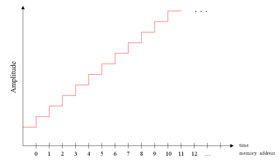
The Data Length parameter should always be greater than or equal to the number of data points in your waveform. It specifies the memory addresses to make available for the waveform, so this is the parameter that will determine how many waveform data values will be output. You can imagine the waveform as a series of data points. Each data value is output for 1 clock until we reach the last value in the waveform cycle. Go to the Data Length section to get a detailed discussion regarding these two parameters.
If the total number of waveform data values is greater than the Data Length, then the last waveform data value that is output is not the one you specify but, instead, is the Nth value, where N equals the Data Length. For example, if your waveform had 100 data values, but your Data Length were 4016 (decimal 64), then the actual last output value would be only the 64th value.
Therefore, assuming there is no delay, for proper waveform output based on your desired values, the necessary condition is:
Number of Data Values
 Data Length
In addition, recall that there are only 4 × 1,048,576 total memory addresses available (maximum memory depth). But, some memory addresses are reserved, so:
AWG252: Number of Data Values
Data Length
3,932,160
AWG452: Number of Data Values
Data Length
7,864,320
Please see the Data Length section for a more detailed discussion regarding the relationship between these two parameters.
Delay
Delay specifies how many memory addresses to keep at the starting value before the waveform starts. For example if your Delay were “5” then the first 5 memory addresses would store values corresponding to the starting data value, and then at the 6th memory address, the waveform would begin. Please note that the delay is counted toward the data length. So if you set data length to 32 and had 30 data values but also set delay to 5, then the last 3 values in your waveform would not be output, since the delay and the data values together exceeded the data length.
Therefore the new Data Length relation becomes:
AWG252: Number of Data Values + Delay
Data Length
3,932,160
AWG452: Number of Data Values + Delay
Data Length
7,864,320
This is the guideline to use for determining proper Data Length.
Marker
The module features three markers, each with different characteristics. They are generated simultaneously with the waveform data, so the markers help you identify when a waveform is output. The marker settings are in the Waveform panel, just below the Data Length box, and allow you to choose when, and for how long, the signals go active.
Markers are useful as diagnostic tools. Markers are ONLY output when there is waveform generation. If you have a marker enabled but you detect no Marker signals, then it means that there is no waveform output.
Marker 1 features 1.8 V TTL (rail-to-rail) logic level. Marker 1 is generated as part of the waveform data, so there is no delay and, in fact, slightly precedes the corresponding waveform output, due to the delay from the latching of the data in the MUXDAC to the analog output. This latency is about 2-3 nanoseconds at the earliest sampling of the waveform data. The signature file records settings for optimal timing of samples, which may result in a waveform output latency up to 3 clocks later than the latency at the earliest sampling opportunity. For instance, if the input clock is 1 GHz, the latency changes by 1 nanosecond at each change in the SEL setting on the Signature panel.
Marker 2 and Marker 3 both feature 3.3 V LVTTL (rail-to-rail) logic levels. These
higher voltage levels are compatible with most instruments, but there is a slight
delay, about 6‑8 nanoseconds, compared with Marker 1.
Markers 2 and 3 can be disabled, and when disabled Marker 3 remains low. To disable
Markers 2 or 3, uncheck the corresponding E enable box in the Waveforms panel.
Marker 2 also features optional reverse polarity if an active low marker is desired.
To make Marker 2 active low, uncheck the P positive polarity box in the Waveforms
panel.